2. Applications of AAO on Al substrate
AAO on Al substrate has honeycomb-like structure, composed with hexagon column of Al2O3, with a circular pore in the center. At the end of the pore, there is a half-sphere shape barrier layer oxide layer in contact with aluminum. The porous oxide film contains mutually parallel cylindrical pores extending from the barrier oxide layer to the film surface. So AAO on Al substrate is suitable to fabricate polymer nanowires or nanotubes.
2.1. Fabrication of polymer nanowires or nanotubes
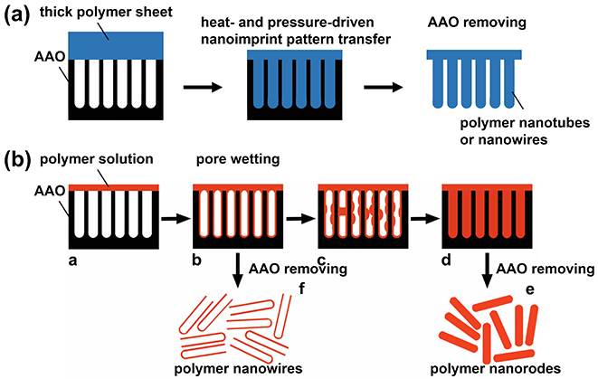
Fig. 2.1 Fabrication of polymer nanowires or nanotubes by (a) heat- and pressure-driven nanoimprint and (b) polymer solution and pore wetting.
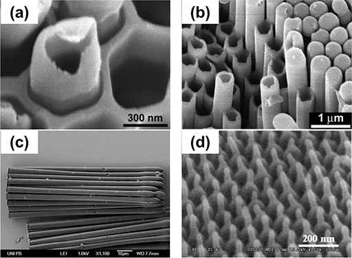
Fig. 2.3 Typical polymer nanostructures fabricated using AAO on Al substrate.
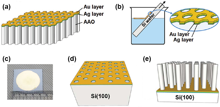
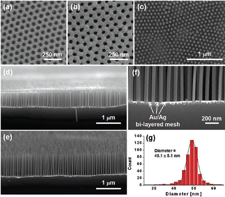
Fig. 2.4 Fabrication of Si Nanowires. (a) sequential sputter depositions of Ag and Au on the surface of AAO membrane; (b) transfer of Au/Ag bilayered metal mesh onto a silicon wafer from the surface of etching solution after removal of AAO membrane and also loosely bound metal nanoparticles from the bottom side of the metal mesh; (c) a photograph of Au/Ag bilayered metal mesh on a Si(100) wafer; (d,e) metal-assisted chemical etching (MaCE) of (100)-oriented silicon wafer for the fabrications of SiNWs.
ACS Nano, 2011, 5, 3222-3229;
ACS Nano, 2011, 5, 5242-5248;
J. Mater. Chem. C, 2013, 1, 5330.
2.4. Fabrication of Metallic Nanopore Arrays
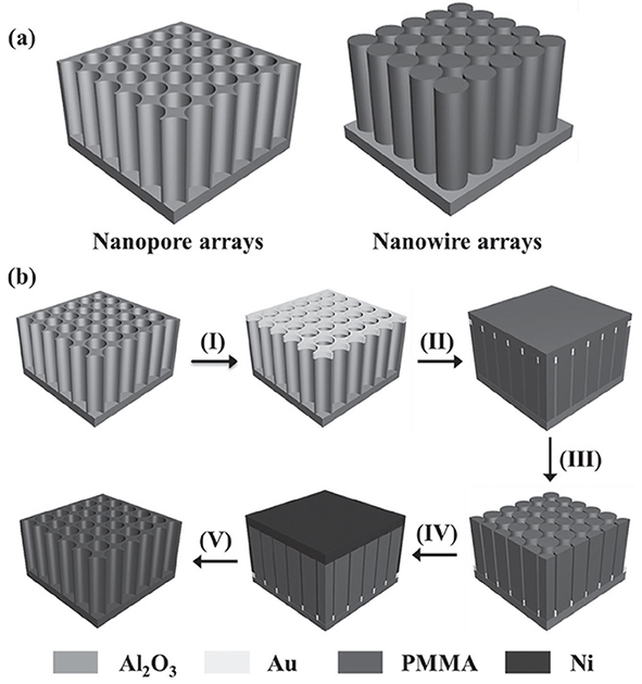
Fig. 2.6 a) Schematic structure of nanopore (left) and nanowire (right) arrays. b) Schematic illustration of the fabrication process of metallic nanopore arrays from the AAO template (Al2O3): gold layer deposition (I), polymer infi ltration (II), template removal (III), Ni electrodeposition (IV), and polymer dissolution (V).
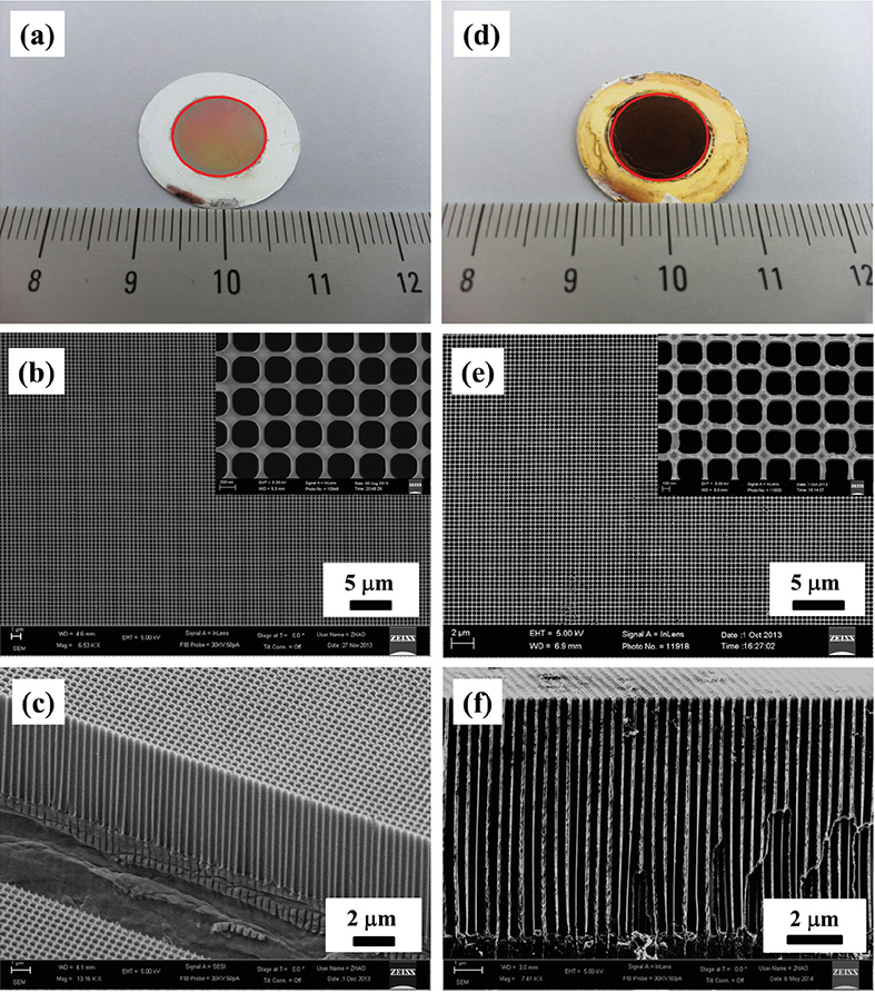 Fig. 2.7 Photographs and SEM images of the original AAO template (a–c) and of the fabricated Ni nanopore arrays (d–f). a,d) Photographs, where the area in the red circle is the nanostructured area. Scale shows lengths in centimeters. b,e) Top and c,f) cross-sectional SEM images; inset of b and e are higher-magnifi cation images.
Adv. Mater. 2014, 26, 7654–7659.
2.5. Fabrication of PDMS Flexible Nanocone Film.
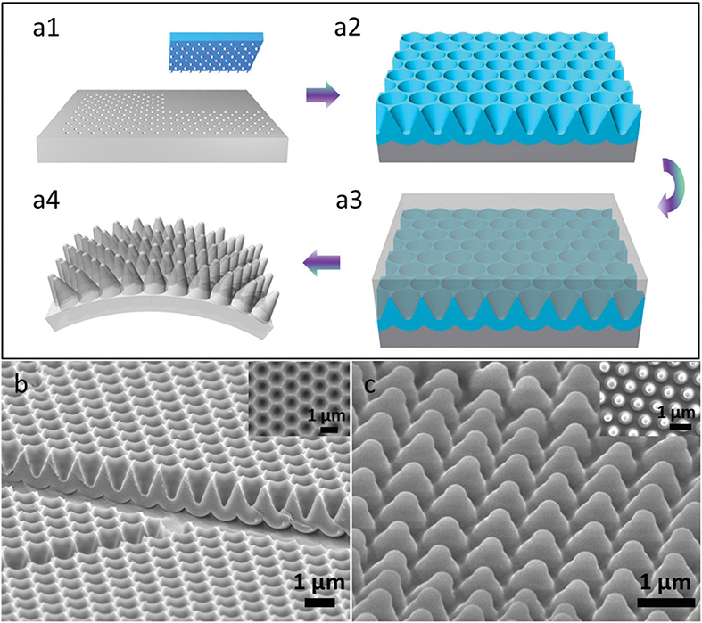
Fig. 2.8 Schematics of nanocone fi lm and SEM images of Au-coated template and PDMS nanocone. a1) A Si mold with hexagonally ordered nanopillars used as imprint mold with four nanoimprint steps. a2) The i-cone array fabricated by a multi-step anodization and wet etching process on the imprinted Al foil. a3) Premixed PDMS poured on Au-coated template followed by a degas and curing process. a4) Regular nanocone on fl exible PDMS after peeling off. b) Aucoated template with 1 μm pitch and 1 μm depth. c) Nanocone with 1 μm pitch and 1 μm depth.
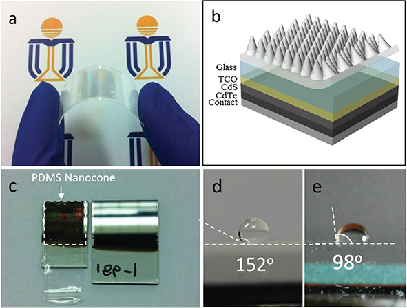
Fig. 2.9 a) Flexible nanocone fi lm. b) Schematic structure of the solar cell device with nanocone PDMS fi lm attached on the top. c) Visual effect of the nanocone AR layer on CdTe devices. The bare sample on the right and the sample with PDMS nanocone on top on the left. d) A drop of water on the nanocone PDMS fi lm showing a large contact angle of 152°. e) A drop of water on the fl at PDMS fi lm showing a contact angle of 98°.
Since the reflectance loss of light leads to inefficient utilization of the incident photons, various anti-reflection (AR) schemes have been developed to achieve high-efficiency solar cell devices. In 2014, Zhiyong Fan team reported utilized a facile molding process to fabricate flexible plastic AR films with three-dimensional (3D) nanocone arrays on the front surface. Fig. 2.8 a1 to a3 shows schematics of the fabrication process. Briefly, an electrochemically polished-clean Al foil was mprinted using a silicon stamp with hexagonally ordered anopillars with height of 200 nm and tunable pitch of 500 nm to 2 μm to produce a nanoindentation array on the surface of the Al foil, as shown in Fig. 2.8 a1. Thereafter, the i-cone array (Fig. 2.8 a2) was fabricated by a multi-step anodization and wet etching process on the imprinted Al foil in an acidic solution with a proper direct-current (DC) voltage. Fig. 2.8b and the inset show scanning electron microscopy (SEM) images of a fabricated i-cone array with cross-sectional and top views, respectively. Fig.2.9a shows a photograph of a fabricated nanocone film naturally attached on a 0.18 mm thick polycarbonate film. Fig. 2.9b schematically illustrates the structure of the solar cell device with nanocone PDMS fi lm attached on the top. In addition to the AR property, it was also found that the PDMS nanocone arrays have superhydrophobic characteristic with large water contact angle.
Reference:
Adv. Mater. 2014, 26, 2805.ACS Nano, 2015, 9, 10287.
2.6. Three-dimensional Nanotube Electrode Arrays.
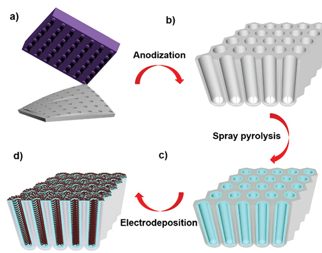
Fig. 2.10 Schematic illustration showing the fabrication process of hierarchical tubular pseudocapacitor electrodes. (a) Nanoimprint process with hexagonal nanopillar Si mold. (b) As-prepared AAO membranes after anodization and Al removal. (c) Ultrasonic spray pyrolysis (USP) deposition of FTO tubular arrays. (d) Hierarchical tubular electrodes achieved by MnO2 electrodeposition.
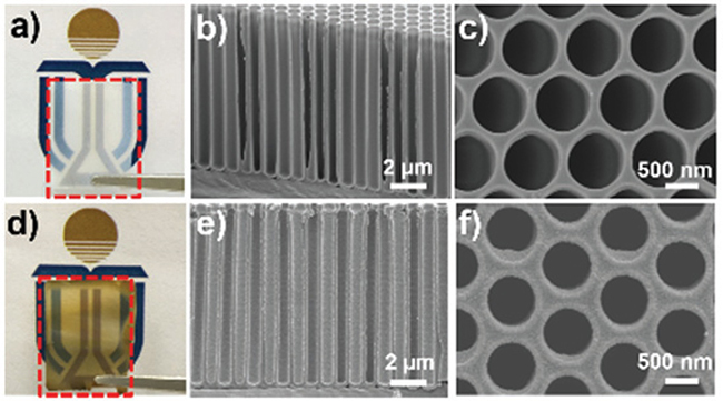
Fig. 2.11 Optical and SEM images of freestanding AAO tubular arrays with the length of 10 μm before USP (a–c). Optical and SEM images of freestanding AAO tubular arrays with the length of 10 μm after USP (d–f ).
Nanoscale, 2016, 8, 13280.